(Hong Kong)

Product Summary
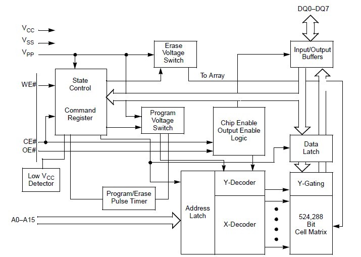
The AM28F512-120EC is a 512 K bit Flash memory organized as 64 Kbytes of 8 bits each. AMDs Flash memories offer the most cost-effective and reliable read/ write non-volatile random access memory. The AM28F512-120EC is packaged in 32-pin PDIP, PLCC, and TSOP versions. It is designed to be reprogrammed and erased in-system or in standard EPROM programmers. The Am28F512 is erased when shipped from the factory. The standard AM28F512-120EC offers access times as fast as 70 ns, allowing operation of high-speed microprocessors without wait states. To eliminate bus contention, the AM28F512-120EC has separate chip enable (CE#) and output enable (OE#) controls.Commands are written to the command register using standard microprocessor write timings. Register contents serve as inputs to an internal state-machine which controls the erase and programming circuitry. During 2 AM28F512-120EC write cycles, the command register internally latches address and data needed for the programming and erase operations. For system design simplification, the AM28F512-120EC is designed to support either WE# or CE# controlled writes. During a system write cycle, addresses are latched on the falling edge of WE# or CE# whichever occurs last. Data is latched on the rising edge of WE# or CE# whichever occurs first. To simplify the following discussion, the WE# pin is used as the write cycle control pin throughout the rest of this text. All setup and hold times are with respect to the WE# signal.
Parametrics
AM28F512-120EC absolute maximum ratings: (1)Storage Temperature: -65°C to +150°C; (2)Plastic Packages: -65°C to +125°C; (3)Ambient Temperature; (4)with Power Applied: -55°C to + 125°C; (5)Voltage with Respect To Ground All pins except A9 and VPP: -2.0 V to +7.0 V; (6)VCC: -2.0 V to +7.0 V; (7)A9: -2.0 V to +14.0 V; (8)VPP: -2.0 V to +14.0 V; (9)Output Short Circuit Current: 200 mA.
Features
AM28F512-120EC features: (1)High performance: 70 ns maximum access time; (2)CMOS Low power consumption; (3)Compatible with JEDEC-standard byte-wide 32-PiEPROM pinouts; (4)10,000 write/erase cycles minimum; (5)Write and erase voltage 12.0 V ±5%; (6)Latch-up protected to 100 mA from -1 V to VCC +1 V; (7)Flasherase Electrical Bulk Chip-Erase: One second typical chip-erase; (8)Flashrite Programming; (9)Command register architecture for microprocessor/microcontroller compatible write interface; (10)On-chip address and data latches; (11)Advanced CMOS flash memory technology: Low cost single transistor memory cell; (12)Automatic write/erase pulse stop timer.
Diagrams