(Hong Kong)

Product Summary
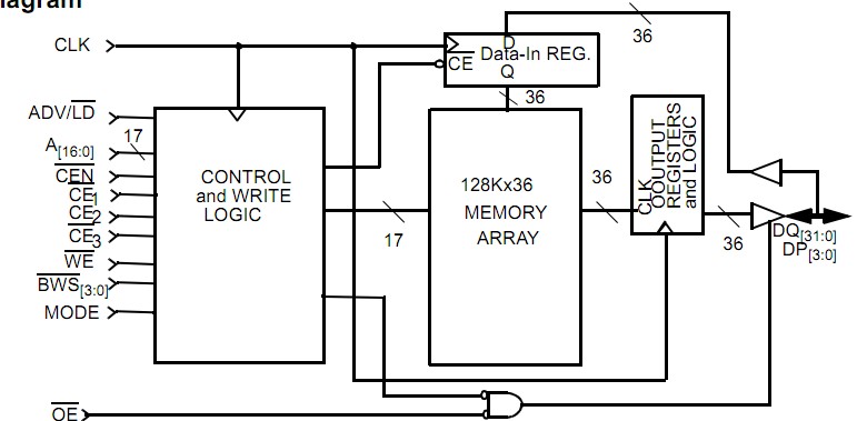
The CY7C1350B-100AC is a 3.3V, 128K by 36 synchronous-pipelined Burst SRAM. The CY7C1350B-100AC is designed specifically to support unlimited true back-to-back Read/Write operations without the insertion of wait states. The CY7C1350B-100AC is equipped with the advanced No Bus Latency (NoBL) logic required to enable consecutive Read/Write operations with data being transferred on every clock cycle. This feature of the CY7C1350B-100AC dramatically improves the throughput of the SRAM, especially in systems that require frequent Write/Read transitions. The CY7C1350B-100AC is pin/func-tionally compatible to ZBT SRAMs IDT71V546, MT55L128L36P, and MCM63Z736.
Parametrics
CY7C1350B-100AC absolute maximum ratings: (1)Storage Temperature: –65 to +150 ℃; (2)Ambient Temperature with Power Applied: –55 to +125 ℃; (3)Supply Voltage on VCC to Relative GND[2]: –0.5 V to +4.6 V; (4)DC Voltage Applied to Outputs[2] in High Z State: –0.5 V to VDD+0.5 V; (5)DC Input Voltage[2]: –0.5 V to VDD+0.5 V; (6)Current into Outputs (LOW): 20 mA; (7)Static Discharge Voltage: >2001V; (8)Latch-Up Current: >200 mA.
Features
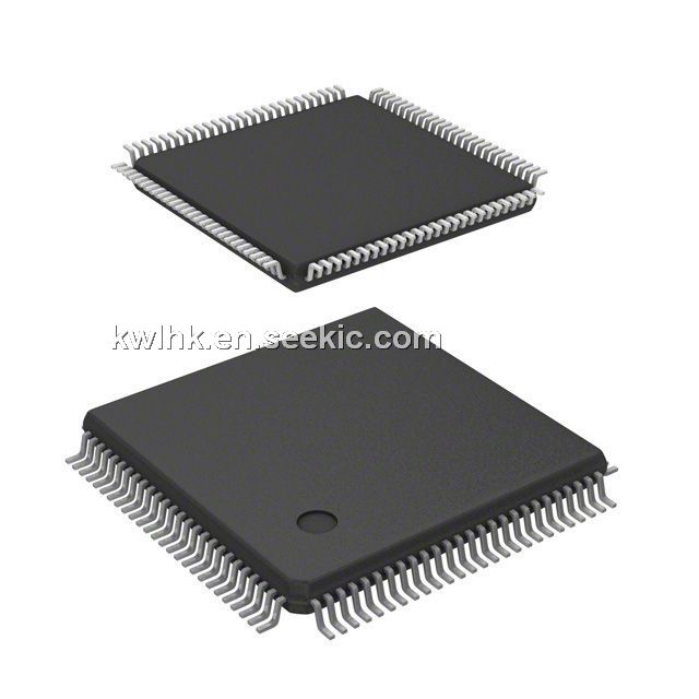
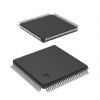
CY7C1350B-100AC features: (1)Pin compatible and functionally equivalent to ZBT devices IDT71V546, MT55L128L36P, and MCM63Z736; (2)Supports 166-MHz bus operations with zero wait states; (3)Internally self-timed output buffer control to eliminate the need to use OE; (4)Fully registered (inputs and outputs) for pipelined operation; (5)Byte Write capability; (6)128K × 36 common I/O architecture; (7)Single 3.3V power supply; (8)Fast clock-to-output times: 3.5 ns; (9)Clock Enable (CEN) pin to suspend operation; (10)Synchronous self-timed writes; (11)Asynchronous output enable; (12)JEDEC-standard 100 TQFP package; (13)Burst Capability—linear or interleaved burst order; (14)Low standby power (17.325 mW max.).
Diagrams