(Hong Kong)

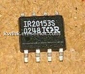
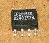
Product Summary
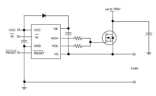
The IR20153S is a high voltage, high speed power MOSFET driver. Proprietary HVIC and latch immune CMOS technologies enable ruggedized monolithic construction. The logic input is compatible with standard CMOS output down to 3.3V. The IR20153S features a high pulse current buffer stage designed for minimum cross-conduction. The IR20153S can be used to drive an N-channel power MOSFET in the high or low side configuration which operates up to 150 volts.
Parametrics
IR20153S absolute maximum ratings: (1)VB High side driver output stage voltage: -5.0 to 170V; (2)VS High side floating supply offset voltage: - 8.0 to 150V; (3)VHO Output voltage gate high connection: VS- 0.3 to VB + 0.3V; (4)VCC Low side fixed supply voltage: -0.3 to 25V; (5)VIN Input voltage (IN and RESET): -0.3 to VCC +0.3V; (6)dV/dt Allowable offset voltage slew rate: 50 V/nsec; (7)TJ Junction temperature: -55 to 150°C; (8)TS Storage temperature: -55 to 150°C; (9)TL Lead temperature (soldering, 10 seconds): 300°C; (10)IQCC VCC supply current: 400 uA.
Features
IR20153S features: (1)Floating channel designed for bootstrap operation; (2)Fully operational up to 150V; (3)Tolerant to negative transient voltage, dV/dt immune; (4)Gate drive supply range from 5V to 20V; (5)Undervoltage lockout; (6)Internal recharge FET for bootstrap refresh; (7)Internal deadtime of 11μs and 0.8μs; (8)CMOS Schmitt-triggered input logic; (9)Output out of phase with input; (10)Reset input; (11)Split pull-up and pull-down gate drive pins; (12)Also available LEAD-FREE (PbF).
Diagrams
| Image | Part No | Mfg | Description |  |
Pricing (USD) |
Quantity | ||||
|---|---|---|---|---|---|---|---|---|---|---|
 |
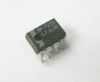
 IR20153S |
Other |
|
Data Sheet |
Negotiable |
|
||||
 |
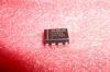
IR20153SPBF |
|
IC DRIVER HI SIDE RECHARGE 8-SOI |
Data Sheet |
Negotiable |
|
||||
|
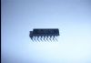
IR20153STRPBF |
|
IC DRIVER HI SIDE RECHARGE 8SOIC |
Data Sheet |
Negotiable |
|
||||