(Hong Kong)

Product Summary
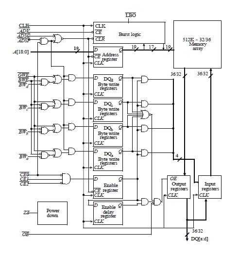
The AS7C33512PFS36A-133TQCALLIANCE is a high-performance CMOS 16-Mbit synchronous Static Random Access Memory (SRAM) device organized as 524,288 words x 32/36. The AS7C33512PFS36A-133TQCALLIANCE incorporates a two-stage register-register pipeline for highest frequency on any given technology. Fast cycle times of 6/7.5 ns with clock access times (tCD) of 3.4/3.8 ns enable 166, and 133 MHz bus frequencies. Three chip enable (CE) inputs permit easy memory expansion. Burst operation is initiated in one of two ways: the controller address strobe (ADSC), or the processor address strobe (ADSP). The AS7C33512PFS36A-133TQCALLIANCE allows subsequent internally generated burst addresses.
Parametrics
AS7C33512PFS36A-133TQCALLIANCE absolute maximum ratings: (1)Power supply voltage relative to GND VDD, VDDQ: -0.5 to +4.6 V; (2)Input voltage relative to GND (input pins)VIN: -0.5 to VDD + 0.5 V; (3)Input voltage relative to GND (I/O pins)VIN: -0.5 to VDDQ + 0.5 V; (4)Power dissipation Pd: 1.8 W; (5)Short circuit output current IOUT: 20 mA; (6)Storage temperature Tstg: -65 to +150°C; (7)Temperature under bias Tbias: -65 to +135°C.
Features
AS7C33512PFS36A-133TQCALLIANCE features: (1)Organization: 524,288 words × 32 or 36 bits; (2)Fast clock speeds to 166 MHz; (3)Fast clock to data access: 3.4/3.8 ns; (4)Fast OE access time: 3.4/3.8 ns; (5)Fully synchronous register-to-register operation; (6)Single-cycle deselect; (7)Asynchronous output enable control; (8)Available in 100-pin TQFP package; (9)Individual byte write and global write; (10)Multiple chip enables for easy expansion; (11)3.3V core power supply; (12)2.5V or 3.3V I/O operation with separate VDDQ; (13)Linear or interleaved burst control; (14)Snooze mode for reduced power-standby; (15)Common data inputs and data outputs.
Diagrams