(Hong Kong)

Product Summary
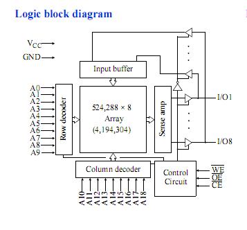
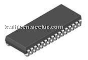
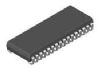
The as7c4096-12jc is a high-performance CMOS 4,194,304-bit Static Random Access Memory (SRAM) device. The as7c4096-12jc is organized as 524,288 words×8 bits. The as7c4096-12jc is designed for memory applications where fast data access, low power, and simple interfacing are desired. When CE the as7c4096-12jc is High the enters standby mode. The standard as7c4096-12jc is guaranteed not to exceed 110/72mW power consumption in CMOS standby mode. All chip inputs and outputs of the as7c4096-12jc are TTL- and CMOS-compatible, and operation is from either a single 3.3V supply. The as7c4096-12jc is available in the JEDEC standard 400-mL, 44-pin SOJ and TSOP 2 packages.
Parametrics
as7c4096-12jc absolute maximum ratings: (1) Voltage on VCC relative to GND Vt1: -1 to +7V; (2) Voltage on any pin relative to GND Vt2: -0.5 to Vcc +0.5V; (3) Power dissipation PD: 1.0W; (4) Storage temperature Tstg: -65 to +150°C; (5) Ambient temperature with Vcc applied Tbias: -55 to +125°C; (6) DC current into outputs (low) IOUT: 20mA.
Features
as7c4096-12jc features: (1) 5V version; (2) Industrial and commercial temperature; (3) Organization: 524,288 words ×8bit; (4) Center power and ground pins; (5) High speed: 10/12/15/20 ns address access time, 5/6/7/8 ns output enable access time; (6) Low power consumption: ACTIVE; (7) Low power consumption: STANDBY; (8) Individual byte read/write controls; (9) Easy memory expansion with CE, OE inputs; (10) TTL- and CMOS-compatible, three-state I/O; (11) 44-pin JEDEC standard packages; (12) ESD protection≥2000 volts; (13) Latch-up current≥100mA.
Diagrams