(Hong Kong)

Product Summary
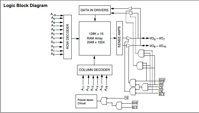
The CY62147CV18LL-70BAI is a high-performance CMOS static RAM organized as 128K words by 16 bits. This device features advanced circuit design to provide ultra-low active current. This is ideal for providing More Battery Life (MoBL) in portable applications such as cellular telephones. The device also has an automatic power-down feature that reduces power consumption by 99% when addresses are not toggling. The device can also be put into standby mode when deselected (CE HIGH) or when CE is LOW and both BLE and BHE are HIGH. The input/output pins (I/O0 through I/O15 ) are placed in a high-impedance state when: deselected (CE HIGH), outputs are disabled (OE HIGH), BHE and BLE are disabled (BHE, BLE HIGH), or during a write operation (CE LOW, and WE LOW).
Parametrics
CY62147CV18LL-70BAI absolute maximum ratings: (1)Storage Temperature: –65°C to +150°C; (2)Ambient Temperature with Power Applied: –55°C to +125°C; (3)Supply Voltage to Ground Potential: –0.5V to +4.6V; (4)DC Voltage Applied to Outputs in High-Z State [4]: –0.5V to VCC + 0.5V; (5)DC Input Voltage [4]: –0.5V to VCC + 0.5V; (6)Output Current into Outputs (LOW): 20 mA; (7)Static Discharge Voltage: > 2001V (per MIL-STD-883, Method 3015); (8)Latch-up Current: > 200 mA.
Features
CY62147CV18LL-70BAI features: (1)Temperature Ranges: Commercial: 0°C to 70°C; Industrial: –40°C to 85°C; Automotive: –40°C to 125°C.; (2)High Speed: 55 ns and 70 ns; (3)Wide voltage range: 2.7V–3.6V; (4)Ultra-low active, standby power; (5)Easy memory expansion with CE and OE features; (6)TTL-compatible inputs and outputs; (7)Automatic power-down when deselected; (8)CMOS for optimum speed/power; (9)Package Available in a standard 44-pin TSOP Type II (forward pinout)package.
Diagrams