(Hong Kong)

Product Summary
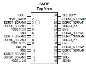
The CYW2560XC is a 12 output buffer. The part has 12 outputs. Designers can configure these outputs to support 3 unbuffered standard SDRAM DIMMs and 2 DDR DIMMs. The CYW2560XC also includes an SMBus interface which can enable or disable each output clock. On power-up, all output clocks are enabled (internal pull-up). It can be used in conjunction with the W250-02 or similar clock synthesizer for the VIA Pro 266 chipset.
Parametrics
CYW2560XC absolute maximum ratings: (1)Supply Voltage to Ground Potential:–0.5 to +7.0V; (2)Storage Temperature:–65 to +150 °C; (3)DC Input Voltage (except BUF_IN): –0.5V to VDD+0.5; (4)Static Discharge Voltage: >2000 V.
Features
CYW2560XC features: (1)One input to 12 output buffer/drivers; (2)Supports up to 2 DDR DIMMs or 3 SDRAM DIMMS; (3)One additional output for feedback; (4)SMBus interface for individual output control; (5)Low skew outputs (< 100 ps); (6)Supports 266 MHz and 333 MHz DDR SDRAM; (7)Dedicated pin for power management support; (8)Space-saving 28-pin SSOP package.
Diagrams