(Hong Kong)

Product Summary
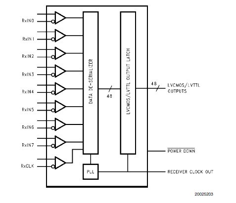
The DS90CR486VS receiver converts eight Low Voltage Differential Signaling (LVDS) data streams back into 48 bits of LVCMOS/LVTTL data. Using a 133MHz clock, the data throughput is 6.384Gbit/s (798Mbytes/s). The multiplexing of data lines provides a substantial cable reduction. Long distance parallel single-ended buses typically require a ground wire per active signal (and have very limited noise rejection capability).
Parametrics
DS90CR486VS absolute maximum ratings: (1)Supply Voltage (VCC): -0.3V to +3.6V; (2)LVCMOS/LVTTL Output Voltage: -0.3V to (VCC + 0.3V); (3)LVDS Receiver Input Voltage: -0.3V to +3.6V; (4)Junction Temperature: +150°C; (5)Storage Temperature: -65°C to +150°C; (6)Lead Temperature (Soldering, 4 sec.): +260°C; (7)Maximum Package Power Dissipation Capacity @ 25° C 100 TQFP Package: 2.9 W.
Features
DS90CR486VS features: (1)Up to 6.384 Gbps throughput; (2)66MHz to 133MHz input clock support; (3)Reduces cable and connector size and cost; (4)Cable Deskew function; (5)DC balance reduces ISI distortion; (6)For point-to-point backplane or cable applications; (7)Low power, 890 mW typ at 133MHz; (8)Flow through pinout for easy PCB design; (9)+3.3V supply voltage; (10)100-pin TQFP package; (11)Conforms to TIA/EIA-644-A-2001 LVDS Standard.
Diagrams
| Image | Part No | Mfg | Description |  |
Pricing (USD) |
Quantity | ||||||||||||
|---|---|---|---|---|---|---|---|---|---|---|---|---|---|---|---|---|---|---|
 |
 DS90CR486VS |
National Semiconductor (TI) |
LVDS Interface IC |
Data Sheet |
|
|
||||||||||||
 |
DS90CR486VS/NOPB |
National Semiconductor (TI) |
LVDS Interface IC |
Data Sheet |
|
|
||||||||||||
|
DS90CR486VSX/NOPB |
National Semiconductor (TI) |
LVDS Interface IC |
Data Sheet |
|
|
||||||||||||
|
DS90CR486VSX |
National Semiconductor (TI) |
LVDS Interface IC |
Data Sheet |
|
|
||||||||||||