(Hong Kong)

Product Summary
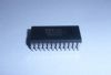
The TC7MBD3245FK is a dual supply, advanced high-speed CMOS 8-bit dual supply voltage interface bus transceiver fabricated with silicon gate CMOS technology. The TC7MBD3245FK is also designed with over voltage tolerant inputs and outputs up to 3.6 V. The direction of data transmission is determined by the level of the DIR input. The enable input (OE ) can be used to disable the device so that the buses are effectively isolated. All inputs are equipped with protection circuits against static discharge or transient excess voltage.
Parametrics
TC7MBD3245FK absolute maximum ratings: (1)Power supply voltage (Note 2)VCCB: -0.5 to 4.6 V; (2)DC input voltage (DIR, OE )VIN: -0.5 to 4.6 V; (3)Input diode current IIK: 50 mA; (4)Output diode current II/OK: ±50 mA, IOUTA: ±25mA; (5)DC output current IOUTB: ±25 mA, ICCA ±50mA; (6)DC VCC/ground current per supply pin ICCB: ±50 mA; (7)Power dissipation PD: 180 mW; (8)Storage temperature Tstg: -65 to 150 °C.
Features
TC7MBD3245FK features: (1)Bidirectional interface between 1.2-V and 1.8-V, 1.2-V and 2.5-V, 1.2-V and 3.3-V, 1.5-V and 2.5-V, 1.5-V and 3.3-V, 1.8-V and 2.5-V, 1.8-V and 3.3-V or 2.5-V and 3.3-V buses; (2)High-speed operation; (3)Output current : IOH/IOL = ±12 mA (min)(VCC = 3.0 V); IOH/IOL = ±9 mA (min)(VCC = 2.3 V); IOH/IOL = ±3 mA (min)(VCC = 1.65 V); IOH/IOL = ±1 mA (min)(VCC = 1.4 V); (4)Latch-up performance: ±300 mA; (5)ESD performance: Machine model ≥ ±200 V, Human body model ≥ ±2000 V; (6)Ultra-small package: VQON24; (7)Low current consumption : Using the new circuit significantly reduces current consumption when OE = “H”; (8)Floating A-bus and B-bus are permitted.
Diagrams