(Hong Kong)

Product Summary
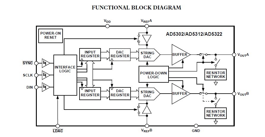
The AD53025JSTP is a buffered voltage output DAC in a 10-lead mSOIC package that operate from a single +2.5 V to +5.5 V supply consuming 230 mA at 3 V. The references for the two DACs are derived from two reference pins (one per DAC). The reference inputs may be configured as buffered or unbuffered inputs. The outputs of the AD53025JSTP may be updated simultaneously using the asynchronous LDAC input. The parts incorporate a power-on-reset circuit that ensures that the DAC outputs power-up to 0 V and remain there until a valid write takes place to the device. The AD53025JSTP contains a powerdown feature that reduces the current consumption of the devices to 200 nA at 5 V (50 nA at 3 V) and provides softwareselectable output loads while in power-down mode. Applications are (1)Portable Battery-Powered Instruments; (2)Digital Gain and Offset Adjustment; (3)Programmable Voltage and Current Sources; (4)Programmable Attenuators.
Parametrics
AD53025JSTP absolute maximum ratings: (1)VDD to GND: -0.3 V to +7 V; (2)Digital Input Voltage to GND: -0.3 V to VDD + 0.3 V; (3)Reference Input Voltage to GND: -0.3 V to VDD + 0.3 V; (4)VOUTA, VOUTB to GND: -0.3 V to VDD + 0.3 V; (5)Operating Temperature Range Industrial (B Version): -40°C to +105°C, Storage Temperature Range: -65°C to +150°C; (6)Lead Temperature, Soldering Vapor Phase (60 sec): 215°C, Infrared (15 sec): 220°C.
Features
AD53025JSTP features: (1)10-Lead mSOIC Package; (2)Micropower Operation: 300 mA @ 5 V (Including Reference Current); (3)Power-Down to 200 nA @ 5 V, 50 nA @ 3 V; (4)+2.5 V to +5.5 V Power Supply; (5)Double-Buffered Input Logic; (6)Guaranteed Monotonic By Design Over All Codes; (7)Buffered/Unbuffered Reference Input Options; (8)0–VREF Output Voltage; (9)Power-On-Reset to Zero Volts; (10)Simultaneous Update of DAC Outputs via LDAC; (11)Low Power Serial Interface with Schmitt-Triggered Inputs; (12)On-Chip Rail-to-Rail Output Buffer Amplifiers.
Diagrams