(Hong Kong)

Product Summary
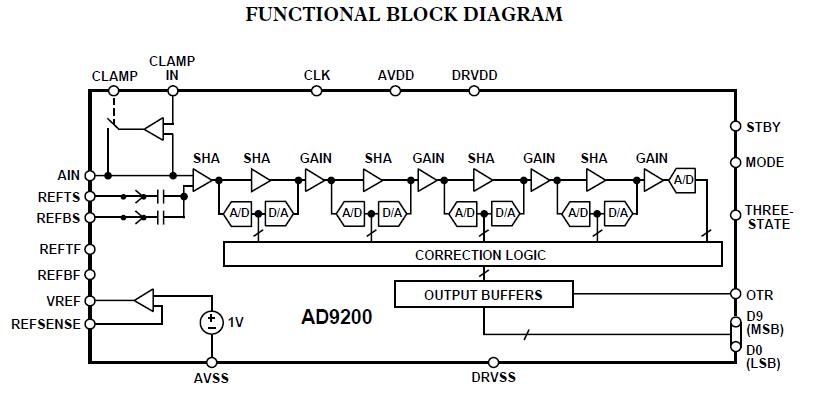
The AD9200JST is a monolithic, single supply, 10-bit, 20 MSPS analog-to-digital converter with an on-chip sample-and-hold amplifier and voltage reference. The AD9200JST uses a multistage differential pipeline architecture at 20 MSPS data rates and guarantees no missing codes over the full operating temperature range. The input of the AD9200JST has been designed to ease the development of both imaging and communications systems. The user can select a variety of input ranges and offsets and can drive the input either single-ended or differentially.
Parametrics
AD9200JST absolute maximum ratings: (1)AVDD, AVSS: -0.3 to +6.5 V; (2)DRVDD, DRVSS: -0.3 to +6.5 V; (3)AVSS, DRVSS: -0.3 to +0.3 V; (4)AVDD, DRVDD: -6.5 to +6.5 V; (5)MODE, AVSS: -0.3 to AVDD +0.3 V; (6)CLK, AVSS: -0.3 to AVDD +0.3 V; (7)Digital Outputs, DRVSS: -0.3 to DRVDD + 0.3 V; (8)AIN, AVSS: -0.3 to AVDD +0.3 V; (9)VREF, AVSS: -0.3 to AVDD +0.3 V; (10)REFSENSE, AVSS: -0.3 to AVDD +0.3 V; (11)REFTF, REFTB, AVSS: -0.3 to AVDD +0.3 V; (12)REFTS, REFBS, AVSS: -0.3 to AVDD +0.3 V; (13)Junction Temperature: +150℃; (14)Storage Temperature: -65 to +150℃; (15)Lead Temperature, 10 sec: +300℃.
Features
AD9200JST features: (1)CMOS 10-Bit, 20 MSPS Sampling A/D Converter; (2)Pin-Compatible with AD876; (3)Power Dissipation: 80 mW (3 V Supply); (4)Operation Between 2.7 V and 5.5 V Supply; (5)Differential Nonlinearity: 0.5 LSB; (6)Power-Down (Sleep) Mode; (7)Three-State Outputs; (8)Out-of-Range Indicator; (9)Built-In Clamp Function (DC Restore); (10)Adjustable On-Chip Voltage Reference; (11)IF Undersampling to 135 MHz.
Diagrams
| Image | Part No | Mfg | Description |  |
Pricing (USD) |
Quantity | ||||
|---|---|---|---|---|---|---|---|---|---|---|
 |
 AD9200JST |
Analog Devices Inc |
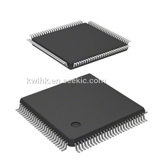
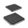
IC ADC 10BIT CMOS 20MSPS 48-LQFP |
Data Sheet |
Negotiable |
|
||||
|
AD9200JSTZ |
Analog Devices Inc |
IC ADC 10BIT CMOS 20MSPS 48-LQFP |
Data Sheet |
Negotiable |
|
||||