(Hong Kong)

Product Summary
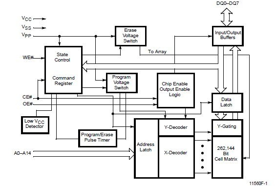
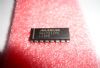
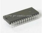
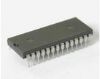
The AM28F256-150PC is a 256 K Flash memory organized as 32 Kbytes of 8 bits each. AMDs Flash memories offer the most cost-effective and reliable read/write nonvolatile random access memory. The AM28F256-150PC is packaged in 32-pin PDIP, PLCC, and TSOP versions. It is designed to be reprogrammed and erased in-system or in standard EPROM programmers. The Am28F256 is erased when shipped from the factory. The AM28F256-150PC is byte programmable using 10 μs programming pulses in accordance with AMDs Flashrite programming algorithm. The typical room temperature programming time of the AM28F256-150PC is a half a second. The entire chip is bulk erased using 10 ms erase pulses according to AMDs Flasherase alrogithm. Typical erasure at room temperature is accomplished in less than one second. The windowed package and the 15-20 minutes required for EPROM erasure using ultra-violet light are eliminated.
Parametrics
AM28F256-150PC absolute maximum ratings: (1)Storage Temperature: -65°C to +150°C; (2)Plastic Packages: -65°C to +125°C; (3)Ambient Temperature with Power Applied: -55°C to + 125°C; (4)Voltage with Respect To Ground All pins except A9 and VPP: -2.0 V to +7.0 V; (5)VCC: -2.0 V to +7.0 V; (6)A9: -2.0 V to +14.0 V; (7)VPP: -2.0 V to +14.0 V; (8)Output Short Circuit Current: 200 mA.
Features
AM28F256-150PC features: (1)High performance: 70 ns maximum access time; (2)CMOS Low power consumption; (3)Compatible with JEDEC-standard byte-wide 32-PiEPROM pinouts — 32-piPDIP; (4)10,000 write/erase cycles minimum; (5)Write and erase voltage 12.0 V ±5%; (6)Latch-up protected to 100 mA from –1 V to VCC +1 V Flasherase Electrical Bulk Chip-Erase; (7)Flashrite Programming; (8)Command register architecture for microprocessor/microcontroller compatible write interface On-chip address and data latches; (9)Advanced CMOS flash memory technology: Low cost single transistor memory cell; (10)Automatic write/erase pulse stop timer.
Diagrams