(Hong Kong)


Product Summary
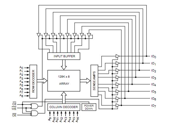
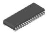
The CY7C1019D-10VXC is a high-performance CMOS static RAM. The CY7C1019D-10VXC is organized as 131,072 words by 8 bits. Easy memory expansion of the CY7C1019D-10VXC is provided by an active LOW Chip Enable (CE1), an active HIGH Chip Enable (CE2), an active LOW Output Enable (OE), and three-state drivers. The CY7C1019D-10VXC has an automatic power-down feature that significantly reduces power consumption when deselected. Writing to the CY7C1019D-10VXC is accomplished by taking Chip Enable One (CE1) and Write Enable (WE) inputs LOW and Chip Enable Two (CE2) input HIGH. Data on the eight I/O pins (I/O0 through I/O7) is then written into the location specified on the address pins.
Parametrics
CY7C1019D-10VXC absolute maximum ratings: (1)Storage Temperature: -65 to +150 ℃; (2)Ambient Temperature with Power Applied: –55 to +125 ℃; (3)Supply Voltage on VCC to relative GND: –0.5 V to +6.0 V; (4)DC Voltage applied to outputs in high Z state: –0.5 V to VCC+0.5 V; (5)DC Input Voltage: –0.5 V to VCC+0.5 V; (6)Current into Outputs (LOW): 20 mA; (7)Static Discharge Voltage: >2001V; (8)Latch-Up Current: >200 mA.
Features
CY7C1019D-10VXC features: (1)Pin and function compatible with CY7C1019D-10VXC; (2)High speed: 10 ns; (3)Low active power; (4)Low CMOS standby power; (5)2.0 V data retention; (6)Automatic power-down when deselected; (7)CMOS for optimum speed/power; (8)Center power/ground pinout; (9)Easy memory expansion with CE and OE options; (10)Functionally equivalent to CY7C1019BV33-10VC; (11)Available in 32-pin 400-mil wide molded SOJ and 32-pin TSOP II packages.
Diagrams