(Hong Kong)

Product Summary
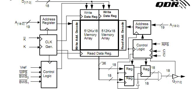
The CY7C1303AV25-167BZC is a 2.5 V Synchronous Pipelined SRAM. The CY7C1303AV25-167BZC is equipped with QDR architecture. QDR architecture of the CY7C1303AV25-167BZC consists of two separate ports to access the memory array. The Read port of the CY7C1303AV25-167BZC has dedicated Data Outputs to support Read operations and the Write Port has dedicated Data inputs to support Write operations. Access to each port of the CY7C1303AV25-167BZC is accomplished through a common address bus. The Read address of the CY7C1303AV25-167BZC is latched on the rising edge of the K clock and the Write address is latched on the rising edge of K clock.
Parametrics
CY7C1303AV25-167BZC absolute maximum ratings: (1)Storage Temperature: –65 to +150 ℃; (2)Ambient Temperature with Power Applied: –55 to +125 ℃; (3)Supply Voltage on VCC to Relative GND[2]: –0.5 V to +3.6 V; (4)DC Voltage Applied to Outputs[2] in High Z State: –0.5 V to VCC + 0.5 V; (5)DC Input Voltage[2]: –0.5 V to VCC + 0.5 V; (6)Current into Outputs (LOW): 20 mA; (7)Static Discharge Voltage: >2001V; (8)Latch-Up Current: >200 mA.
Features
CY7C1303AV25-167BZC features: (1)Separate independent Read and Write data ports; (2)167-MHz Clock for high bandwidth; (3)2-Word Burst on all accesses; (4)Double Data Rate (DDR) interfaces on both Read and Write Ports; (5)Two input clocks (K and K) for precise DDR timing; (6)Two output clocks (C and C) account for clock skew and flight time mismatching; (7)Single multiplexed address input bus latches address inputs for both Read and Write ports; (8)Separate Port Selects for depth expansion; (9)Synchronous internally self-timed writes; (10)2.5V core power supply with HSTL Inputs and Outputs; (11)13 × 15 × 1.4 mm 1.0-mm pitch fBGA package, 165 ball; (12)Expanded HSTL output voltage (1.4V–1.9V); (13)JTAG Interface; (14)Variable Impedance HSTL.
Diagrams