(Hong Kong)

Product Summary
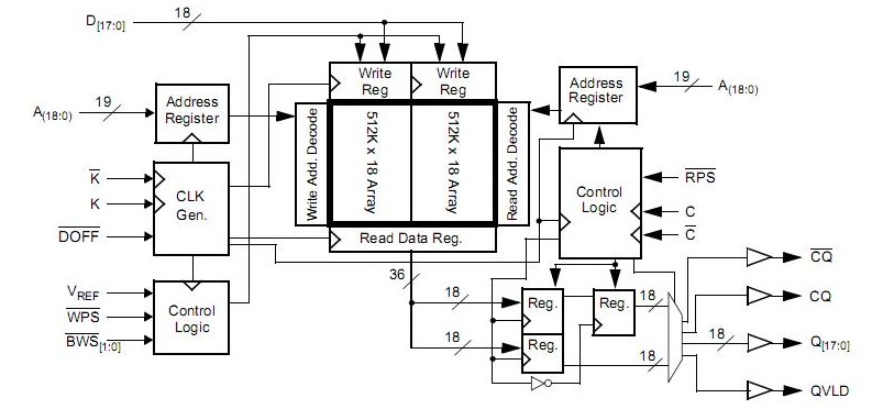
The CY7C131-35JCT is a 1.8V Synchronous Pipelined SRAM. The CY7C131-35JCT consists of two separate ports to access the memory array. The read port has dedicated Data Outputs to support read operations and the Write Port has dedicated Data Inputs to support write operations. The CY7C131-35JCT has separate data inputs and data outputs to completely eliminate the need to “turn-around”the data bus required with common IO devices.
Parametrics
CY7C131-35JCT absolute maximum ratings: (1)Storage Temperature:–65℃ to +150℃; (2)Ambient Temperature with Power Applied:–55℃ to +125℃; (3)Supply Voltage on VDD Relative to GND:–0.5V to +2.9V; (4)Supply Voltage on VDDQ Relative to GND:–0.5V to +VDD; (5)DC Voltage Applied to Outputs in High Z State:–0.5V to VDDQ + 0.3V; (6)DC Input Voltage:–0.5V to VDD + 0.3V; (7)Current into Outputs (LOW):20 mA; (8)Static Discharge Voltage:> 2001V(MIL-STD-883, Method 3015); (9)Latch up Current: > 200 mA.
Features
CY7C131-35JCT features: (1)Two input clocks (K and K) for precise DDR timing; (2)SRAM uses rising edges only; (3)Two input clocks for output data (C and C) to minimize clock; (4)skew and flight time mismatches; (5)Echo clocks (CQ and CQ) simplify data capture in high speed systems; (6)Single multiplexed address input bus latches address inputs for both read and write ports; (7)Separate Port Selects for depth expansion; (8)Synchronous internally self-timed writes; (9)Available in x 8, x 9, x 18, and x 36 configurations; (10)Full data coherency, providing most current data; (11)Core VDD = 1.8V (±0.1V); I/O VDDQ = 1.4V to VDD; (12)Available in 165 ball FBGA package (13 x 15 x 1.4 mm); (13)Offered in both Pb-free and non-Pb-free packages; (14)Variable drive HSTL output buffers; (15)JTAG 1149.1 compatible test access port; (16)Delay Lock Loop (DLL) for accurate data placement.
Diagrams