(Hong Kong)

Product Summary
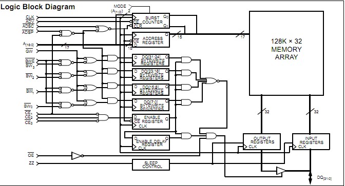
The CY7C1339-133AC is a 3.3V, 64K by 32 synchronous-pipelined cache SRAM. The CY7C1339-133AC is designed to support zero wait state secondary cache with minimal glue logic. The CY7C1339-133AC pins can operate at either the 2.5V or the 3.3V level. The I/O pins of the CY7C1339-133AC are 3.3V tolerant when VDDQ=2.5V. All synchronous inputs pass through input registers controlled by the rising edge of the clock. All data outputs pass through output registers controlled by the rising edge of the clock. Max-imum access delay from the clock rise is 4.2 ns (166-MHz device). The CY7C1339-133AC supports either the interleaved burst sequence used by the Intel Pentium processor or a linear burst sequence used by processors such as the PowerPC.
Parametrics
CY7C1339-133AC absolute maximum ratings: (1)Storage Temperature: –65 to +150 ℃; (2)Ambient Temperature with Power Applied: –55 to +125 ℃; (3)Supply Voltage on VCC to Relative GND[2]: –0.5 V to +4.6 V; (4)DC Voltage Applied to Outputs[2] in High Z State: –0.5 V to VCC + 0.5 V; (5)DC Input Voltage[2]: –0.5 V to VCC + 0.5 V; (6)Current into Outputs (LOW): 20 mA; (7)Static Discharge Voltage: >2001V; (8)Latch-Up Current: >200 mA.
Features
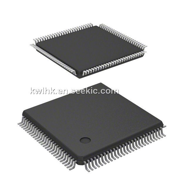
CY7C1339-133AC features: (1)Supports 100-MHz bus for Pentium and PowerPC; (2)operations with zero wait states; (3)Fully registered inputs and outputs for pipelined operation; (4)128K × 32 common I/O architecture; (5)3.3V core power supply; (6)2.5V / 3.3V I/O operation; (7)Fast clock-to-output times: 3.5 ns; (8)User-selectable burst counter supporting Intel Pentium interleaved or linear burst sequences; (9)Separate processor and controller address strobes; (10)Synchronous self-timed writes; (11)Asynchronous output enable; (12)Offered in JEDEC-standard 100-pin TQFP and 119-ball BGA packages; (13)“ZZ” Sleep Mode and Stop Clock options.
Diagrams