(Hong Kong)

Product Summary
The CYW3110XC is a FTG for VIA Pro-266 DDR chipset. The clock driver serial protocol supports byte/word write, byte/word read, block write and block read operations from the controller. The CYW3110XC features a two-pin, serial data interface that can be used to configure internal register settings that control particular device functions.
Parametrics
CYW3110XC absolute maximum ratings: (1)Voltage on any pin with respect to GND:–0.5 to +7.0 V; (2)Storage Temperature:–65 to +150 °C; (3)Ambient Temperature under Bias:–55 to +125 °C; (4)Operating Temperature: 0 to +70 °C; (5)Input ESD Protection: 2 (min.) kV.
Features
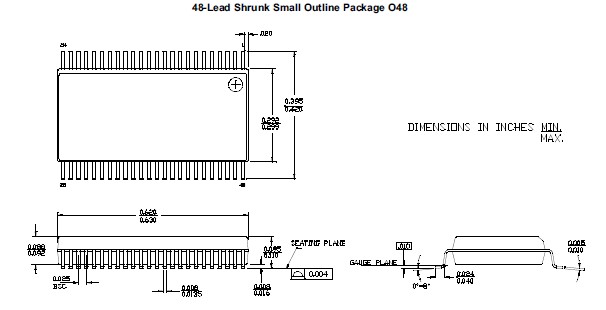
CYW3110XC features: (1)Maximized EMI Suppression using Cypress抯 Spread Spectrum Technology; (2)System frequency synthesizer for VIA Pro-2000; (3)Programmable clock output frequency with less than 1 MHz increment; (4)Integrated fail-safe Watchdog Timer for system recovery; (5)Automatically switch to HW selected or SW programmed clock frequency when Watchdog Timer time-out; (6)Capable of generate system RESET after a Watchdog Timer time-out occurs or a change in output frequency via SMBus interface; (7)Support SMBus byte read/write and block read/ write operations to simplify system BIOS development; (8)Vendor ID and Revision ID support; (9)Programmable drive strength for CPU and PCI output clocks; (10)Programmable output skew between CPU, AGP and PCI; (11)Three copies of CPU output; (12)Nine copies of PCI output; (13)One 48 MHz output for USB; (14)One 24 MHz or 48 MHz output for SIO; (15)Two buffered reference outputs; (16)Three copies of APIC output; (17)Supports frequencies up to 200MHz; (18)SMBus Interface for programming; (19)Power management control inputs; (20)Available in 48-pin SSOP.
Diagrams