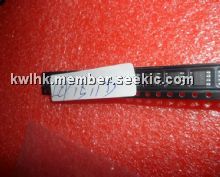
Product Summary
This device LCP1511D has been especially designed to protect subscriber line card interfaces (SLIC) against transient overvoltages.
Positive overloads are clipped with 2 diodes.Negative surges are suppressed by 2 thyristors,their breakdown voltage being referenced to VBAT through the gate.
LCP1511D presents a very low gate triggering current (IGT) in order to reduce the current con-sumption on printed circuit board during the firingphase.
A particular attention has been given to the internalwire bonding. The "4-point" configuration ensuresreliable protection, eliminating the overvoltage in-troduced by the parasitic inductances of the wiring(Ldi/dt), especially for very fast transients.
Parametrics
The absolute maximum ratings of LCP1511D are (1)Maximum gate current (half sine wave tp = 10ms):2A; (2)Maximum voltage LINE / GROUND:-100V; (3)Maximum voltage GATE / LINE:-80V; (4)Storage temperature range:-55 to + 150°C; (5)Maximum junction temperature:150°C; (6)Maximum lead temperature for soldering during 10s:260°C
Features
The features of LCP1511D can be summarized as (1)DUAL PROGRAMMABLE TRANSIENT SUP-PRESSOR.; (2)WIDE NEGATIVE FIRING VOLTAGE RANGE :VMGL = -80V max.; (3)LOW DYNAMIC SWITCHING VOLTAGES :VFP and VDGL.; (4)LOW GATE TRIGGERING CURRENT :IGT = 5mA max.; (5)PEAK PULSE CURRENT :IPP = 30A for 10/1000μs surge.; (6)HOLDING CURRENT :IH = 150mA.
Diagrams
<P><IMG alt="LCP1511D Pin Configuration" src="http://www.seekic.com/uploadfile/ic-mfg/20128120554772.jpg" border=0></P>
| Image | Part No | Mfg | Description |  |
Pricing (USD) |
Quantity | ||||
|---|---|---|---|---|---|---|---|---|---|---|
 |
 LCP1511D |
 Other |
 |
 Data Sheet |
 Negotiable |
|
||||
 |
 LCP1511DRL |
 STMicroelectronics |
 TVS Diode Arrays Dual Program TVS |
 Data Sheet |
 Negotiable |
|
||||
 (Hong Kong)


