(Hong Kong)

Product Summary
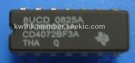
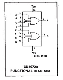
The CD4072BF3A OR gate provides the system designer with direct implementation of the positive-logic OR function and supplement the existing family of CMOS gates. The CD4072BF3A is supplied in 14-lead hermetic dual-in-line ceramic packages (F3A suffix), 14-lead dual-in-line plastic packages (E suffix), 14-lead small-outline packages (M, MT, M96, and NSR suffixes), and 14-lead thin shrink small-outline packages (PW and PWR suffixes).
Parametrics
CD4072BF3A absolute maximum ratings: (1)DC Supply Voltage Range, (VDD): -0.5V to +20V; (2)Input Voltage Range, All Inputs: -0.5V to VDD +0.5V; (3)DC Input Current, Any One Input: ±10mA; (4)Operating Temperature Range: -55℃ to +125℃; (5)Storage Temperature Range (TSTG): -65℃ to +150℃; (6)Lead Temperature (During Soldering): +265℃.
Features
CD4072BF3A features: (1)Medium Speed Operation: tPHL, tPLH = 60ns (typ) at 10V; (2)100% Tested for Quiescent Current at 20V; (3)Maximum Input Current of 1μA at 18V Over Full Pack-age Temperature Range; 100nA at 18V and +25℃; (4)Standardized Symmetrical Output Characteristics; (5)Noise Margin (Over Full Package Temperature Range): 1V at VDD = 5V; 2V at VDD = 10V; 2.5V at VDD = 15V; (6)5V, 10V and 15V Parametric Ratings; (7)Meets All Requirements of JEDEC Tentative Standard No. 13B, “Standard Specications for Description of ‘B’ Series CMOS Devices”.
Diagrams
 |
 CD4000B |
Other |
|
Data Sheet |
Negotiable |
|
||||
|
CD4000BMS |
Other |
|
Data Sheet |
Negotiable |
|
||||
|
CD4001BC |
Other |
|
Data Sheet |
Negotiable |
|
||||
 |
CD4001BCM |
|
IC GATE NOR BUFF QUAD 2IN 14SOIC |
Data Sheet |
Negotiable |
|
||||
|
CD4001BCMX |
|
IC GATE NOR QUAD 2INPUT 14-SOIC |
Data Sheet |
Negotiable |
|
||||
 |
CD4001BCN |
|
IC GATE NOR BUFF QUAD 2IN 14-DIP |
Data Sheet |
Negotiable |
|
||||