(Hong Kong)


Product Summary
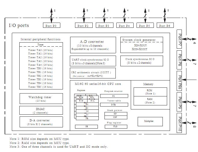
The M30621FCMGP is a single-chip microcomputer built using the high-performance silicon gate CMOS process using a M16C/60 Series CPU core and are packaged ina 80-pin plastic molded QFP. The M30621FCMGP operates using sophisticated instructions featuring a high level of instruction efficiency. With 1M bytes of address space, the device is capable of execut-ing instructions at high speed.
Parametrics
M30621FCMGP absolute maximum ratings: (1)Vcc, Supply voltage: 2.2 to 3.6V; (2)AVcc, Analog supply voltage: Vcc V; (3)Vss, Supply voltage: 0V; (4)AVss, Analog supply voltage: 0V.
Features
M30621FCMGP features: (1)Memory capacity: ROM (See Figure 1.1.3. ROM Expansion)RAM 10K to 20K bytes; (2)Shortest instruction execution time: 100ns (f(XIN)=10MHZ, VCC=2.7V to 3.6V)142.9ns (f(XIN)=7MHZ, VCC=2.2V to 3.6V, with software one-wait); (3)Supply voltage: 2.7V to 3.6V (f(XIN)=10MHZ, without software wait)2.4V to 2.7V (f(XIN)= 7MHZ, without software wait)2.2V to 2.4V (f(XIN)= 7MHZ, with software one-wait); (4)Low power consumption: 28.5mW ( f(XIN)=10MHZ, with software one-wait, VCC = 3V); (5)Interrupts: 25 internal and 5 external interrupt sources, 4 softwareinterrupt sources; 7 levels (including key input interrupt); (6)Multifunction 16-bit timer: 5 output timers + 6 input timers (3 for timer function only); (7)Serial I/O: 5 channels (2 for UART or clock synchronous, 1 for UART, 2 for clock synchronous); (8)DMAC: 2 channels (trigger: 24 sources); (9)A-D converter: 10 bits X 8 channels (Expandable up to 10 channels); (10)D-A converter: 8 bits X 2 channels; (11)CRC calculation circuit: 1 circuit; (12)Watchdog timer: 1 line; (13)Programmable I/O: 70 lines; (14)Input port: 1 line (P85 shared with NMI pin); (15)Clock generating circuit: 2 built-in clock generation circuits.
Diagrams