(Hong Kong)

Product Summary
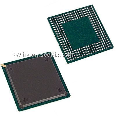
The SSTE32882HLBAKG is a 1.35V/1.5V registering clock driver. The device has two basic modes of operation associated with the Quad Chip Select Enable (QCSEN) input. It is available in a 176-ball BGA with 0.65mm ball pitch in a 11 x 20 grid. It is also available in a 176-ball Thin-Profile Fine-Pitch BGA with 0.65mm ball pitch in an 8x22 grid. The device pinout supports outputs on the outer two left and right columns to support easy DIMM signal routing. The SSTE32882HLBAKG operates from a differential clock (CK and CK). Data are registered at the crossing of CK going high, and CK going low.
Parametrics
SSTE32882HLBAKG absolute maximum ratings: (1)Supply voltage: –0.4 to +1.975 V; (2)Receiver input voltage: -0.4 to Vcc+0.5 V; (3)Reference voltage: -0.4 to Vcc+0.5 V; (4)Driver output voltage: -0.4 to Vcc+0.5 V; (5)Input clamp current: -50 mA; (6)Output clamp current: +/-50 mA; (7)Package Thermal Impedance, Junction-to-Case: 16.2 °C/W; (8)storage temperature: -65 to +150 °C.
Features
SSTE32882HLBAKG features: (1)Pinout optimizes DDR3 RDIMM PCB layout; (2)1-to-2 Register Outputs and 1-to-4 Clock Pair Outputs support stacked DDR3 RDIMMs; (3)Phase Lock Loop clock driver for buffering one differential clock pair (CK and CK) and distributing to four differential outputs; (4)Supports LVCMOS switching levels on the RESET and MIRROR inputs; (5)Checks priority on DIMM-independent data inputs; (6)Supports dynamic 1T/3T timing transaction and output inversion feature for improved timing performance during normal operations and MRS command pass-through; (7)Supports CKE Power Down operation modes; (8)Supports Quad Chip Select operation features; (9)RESET input disables differential input recievers, resets all registers, and disables all output drivers except ERROUT and QnCKEn; (10)Provides access to internal control words for configuring the device features and adapting in different RDIMM and system applications; (11)Latch-up performance exceeds 100mA; (12)ESD > 2000V per MIL-STD883, Method 3015; ESD > 200V using machine model (c = 200pF, R = 0); (13)Available in 176 Ball Grid Array package.
Diagrams

| Image | Part No | Mfg | Description |  |
Pricing (USD) |
Quantity | ||||
|---|---|---|---|---|---|---|---|---|---|---|
 |
 SSTE32882HLBAKG |
Other |
|
Data Sheet |
Negotiable |
|
||||
|
SSTE32882HLBAKG8 |
Other |
|
Data Sheet |
Negotiable |
|
||||