(Hong Kong)

Product Summary
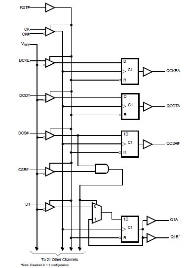
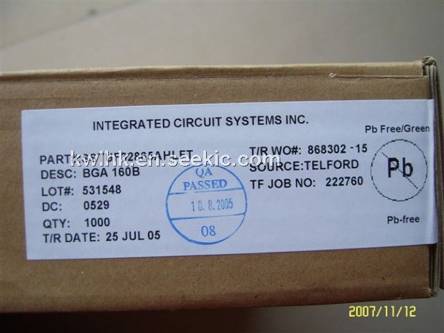
The SSTUF32865AHLFT is a 25-bit 1:1 or 14-bit 1:2 configurable registered buffer. The SSTUF32865AHLFT is designed for 1.7-V to 1.9-V VDD operation. All clock and data inputs are compatible with the JEDEC standard for SSTL_18. The control inputs are LVCMOS. All outputs are 1.8-V CMOS drivers that have been optimized to drive the DDR-II DIMM load. The SSTUF32865AHLFT operates from a differential clock (CK and CK#). Data are registered at the crossing of CK going high, and CK# going low. The C0 input controls the pinout configuration of the 1:2 pinout from A configuration (when low) to B configuration (when high). The C1 input controls the pinout configuration from 25-bit 1:1 (when low) to 14-bit 1:2 (when high). Applications are (1)DDR2 Memory Modules; (2)Provides complete DDR DIMM solution with ICS97U877; (3)Ideal for DDR2 400, 533 and 667.
Parametrics
SSTUF32865AHLFT absolute maximum ratings: (1)Storage Temperature: -65°C to +150°C; (2)Supply Voltage: -0.5V to 2.5V; (3)Input Voltage: -0.5V to +2.5V; (4)Output Voltage: -0.5V to VDD + 0.5V; (5)Input Clamp Current: ±50 mA; (6)Output Clamp Current: ±50mA; (7)Continuous Output Current: ±50mA; (8)VDD or GND Current/Pin: ±100mA; (9)Package Thermal Impedance3: 36°C.
Features
SSTUF32865AHLFT features: (1)25-bit 1:1 or 14-bit 1:2 configurable registered buffer; (2)Supports SSTL_18 JEDEC specification on data inputs and outputs; (3)Supports LVCMOS switching levels on C0, C1 and RESET# inputs; (4)Low voltage operation VDD = 1.7V to 1.9V; (5)Available in 96 BGA package; (6)Drop-in replacement for ICSSSTUF32866; (7)Green packages available.
Diagrams