(Hong Kong)

Product Summary
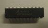
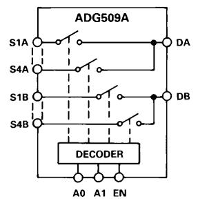
The ADG509AKN is a CMOS monolithic analog multiplexer with eight channels and dual four channels, respec-tively. The ADG509AKN switches one of eight inputs to a common output, depending on the state of three binary addresses and an enable input. It is designed on an enhanced LC2MOS process that gives an increased signal capability of VSS to VDD and enables operation over a wide range of supply voltages. The device can comfortably operate anywhere in the 10.8 V to 16.5 V single- or dual-supply range.
Parametrics
ADG509AKN absolute maximum ratings: (1)VDD to VSS: 44 V; (2)VDD to GND: 32 V; (3)VSS to GND: –32 V; (4)Analog Inputs1, Voltage at S, D: VSS - 2 V to VDD + 2 V or 20 mA, whichever occurs first; (5)Continuous Current, S or D: 20 mA; (6)Pulsed Current S or D, 1 ms Duration, 10% Duty Cycle: 40 mA; (7)Digital Inputs, Voltage at A, EN: VSS - 4 V to VDD + 4 V or 20 mA, whichever occurs first; (8)Power Dissipation (Any Package) Up to 75℃: 470 mW; (9)Derates Above 75℃ by: 6 mW/℃; (10)Operating Temperature: Commercial (K Version): -40℃ to +85℃; Industrial (B Version): -40℃ to +85℃; Extended (T Version): -55℃ to +125℃; (11)Storage Temperature Range: -65℃ to +150℃.
Features
ADG509AKN features: (1)44 V supply maximum rating; (2)VSS to VDD analog signal range; (3)Single-/dual-supply specifications; (4)Wide supply range: 10.8 V to 16.5 V; (5)Extended plastic temperature range: -40℃ to +85℃; (6)Low power dissipation: 28 mW maximum; (7)Low leakage: 20 pA typical; (8)Available in 16-lead DIP/SOIC and 20-lead PLCC/LCC packages; (9)Superior alternative toDG508A, HI-508.
Diagrams
| Image | Part No | Mfg | Description |  |
Pricing (USD) |
Quantity | ||||||||||||||||||
|---|---|---|---|---|---|---|---|---|---|---|---|---|---|---|---|---|---|---|---|---|---|---|---|---|
 |
 ADG509AKN |
|
IC MULTIPLEXER DUAL 4X1 16DIP |
Data Sheet |
|
|
||||||||||||||||||
|
ADG509AKNZ |
|
IC MULTIPLEXER DUAL 4X1 16DIP |
Data Sheet |
|
|
||||||||||||||||||