(Hong Kong)


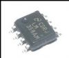
Product Summary
The IDT74FCT388915T100PY is a 3.3V low skew pll-based cmos clock driver. The IDT74FCT388915T100PY uses phase-lock loop technology to lock the frequency and phase of outputs to the input reference clock. The IDT74FCT388915T100PY provides low skew clock distribution for high performance PCs and workstations. One of the outputs is fed back to the PLL at the FEEDBACK input resulting in essentially zero delay across the device. The PLL consists of the phase/frequency detector, charge pump, loop filter and VCO.
Parametrics
IDT74FCT388915T100PY absolute maximum ratings: (1)VTERM(2)Terminal Voltage with Respect to GND: –0.5 to +4.6 V; (2)VTERM(3)Terminal Voltage with Respect to GND: –0.5 to +7.0 V; (3)VTERM(4)Terminal Voltage with Respect to GND: –0.5 to VCC +0.5 V; (4)TA Operating Temperature: –55 to +125 °C; (5)TBIAS Temperature Under Bias: –65 to +135 °C; (6)TSTG Storage Temperature: –65 to +150 °C; (7)IOUT DC Output Current: –60 to +60 mA.
Features
IDT74FCT388915T100PY features: (1)Max. output frequency: 150MHz; (2)Pin and function compatible with FCT88915T, MC88915T; (3)5 non-inverting outputs, one inverting output, one 2x output, one ¸2 output; all outputs are TTL-compatible; (4)3-State outputs; (5)Output skew < 350ps (max.); (6)Duty cycle distortion < 500ps (max.); (7)Part-to-part skew: 1ns (from tPD max. spec); (8)32/–16mA drive at CMOS output voltage levels; (9)VCC = 3.3V ± 0.3V; (10)Inputs can be driven by 3.3V or 5V components; (11)Available in 28 pin PLCC, LCC and SSOP packages.
Diagrams