(Hong Kong)

Product Summary
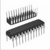
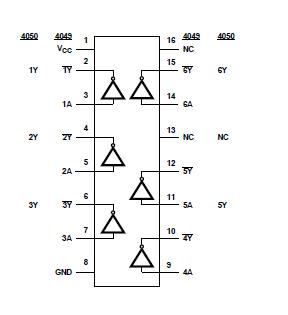
The CD54HC4050F3A is a Buffer/Converter with 6-CH Non-Inverting CMOS 16-Pin CDIP Tube. It is fabricated with high-speed silicon gate technology. The CD54HC4050F3A has a modified input protection structure that enables these parts to be usedas logic level translators which convert high-level logic to a lowlevel logic while operating off the low-level logic supply.
Parametrics
CD54HC4050F3A absolute maximum ratings: (1)DC Supply Voltage, VCC: –0.5V to 7V; (2)Input Voltage Range: –0.5V to 16V; (3)DC Input Diode Current, IIK For VI < –0.5V: –20mA; (4)DC Output Diode Current, IOK For VO < –0.5V or VO > VCC + 0.5V: ±20mA; (5)Operating Conditions Temperature Range (TA): –55℃ to 125℃; (6)Package Thermal Impedance, θJA: 67℃/W.
Features
CD54HC4050F3A features: (1)Typical Propagation Delay: 6ns at VCC = 5V, CL = 15pF, TA = 25℃; (2)High-to-Low Voltage Level Converter for up to Vl = 16V; (3)Fanout (Over Temperature Range) Standard Outputs: 10 LSTTL Loads; (4)Bus Driver Outputs: 15 LSTTL Loads; (5)Wide Operating Temperature Range: -55℃ to 125℃; (6)Balanced Propagation Delay and Transition Times; (7)Significant Power Reduction Compared to LSTTL Logic ICs.
Diagrams
 |
 CD54 |
Other |
|
Data Sheet |
Negotiable |
|
||||
|
CD54/74HC161 |
Other |
|
Data Sheet |
Negotiable |
|
||||
|
CD54/74HC163 |
Other |
|
Data Sheet |
Negotiable |
|
||||
|
CD54/74HC192 |
Other |
|
Data Sheet |
Negotiable |
|
||||
|
CD54/74HC193 |
Other |
|
Data Sheet |
Negotiable |
|
||||
|
CD54/74HC240 |
Other |
|
Data Sheet |
Negotiable |
|
||||